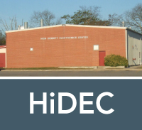
High Density Electronics Center (HiDEC)
Since its inception, HiDEC personnel have pursued a program of excellence in research and education, which has earned the program an international reputation.
Established in 1991, the HiDEC facilities includes nearly 6,000 square feet of clean room space which houses conventional MCM processing on five-inch wafers, deposition and photolithographic definition of thin film materials, and package assembly.
HiDEC research includes all aspects of advanced electronic packaging, including, but not limited to, such areas as materials synthesis, low cost MCM design techniques, flip chip die attachment, flexible substrates, integrated passive components, low temperature cofired ceramic, wideband electrical characterization, analytical and lifetime testing.
For more information, please contact:
Errol Porter
479-575-2519
evporte@uark.edu